


The simple, plain-English guide to how silicon carbide makes microchips for the semiconductor industry
How are microchips made? Well, to start, let’s look at the famous quote by science fiction author Arthur C. Clarke:
“Any sufficiently advanced technology is indistinguishable from magic.”
We live in an electronic world that grows exponentially, and that technology is possible thanks in large part to the rapid innovation coming from microchips. They’re the brains of our electronics. And if you squint, the art of producing microchips for the semiconductor industry does indeed look like magic. Each microchip—roughly the size of a fingernail—is home to billions of transistors.
Here’s how the incredible process works, from start to finish. And stay tuned until the end, because you’ll also find out how UNITED GRINDING surface and profile grinding machines and cylindrical grinding machines can help semiconductor manufacturers make chips faster and better than ever.


It all starts with silicon.
Silicon (Si, atomic number 14) is a semiconductor, meaning it resides in the sweet spot between insulators on one side and conductors on the other. And because it’s typically found in sand, it’s one of the most prevalent elements on planet earth.
But silicon is also usually bound with oxygen, so before we can get our bouncing baby microchips, those two elements need to be separated. This is why we take our silicon-rich sand, combine it with carbon and melt it in crucibles. This produces carbon monoxide and (most importantly for our purposes), 99% pure silicon.
Here comes the seed crystal.
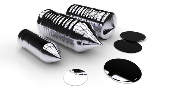
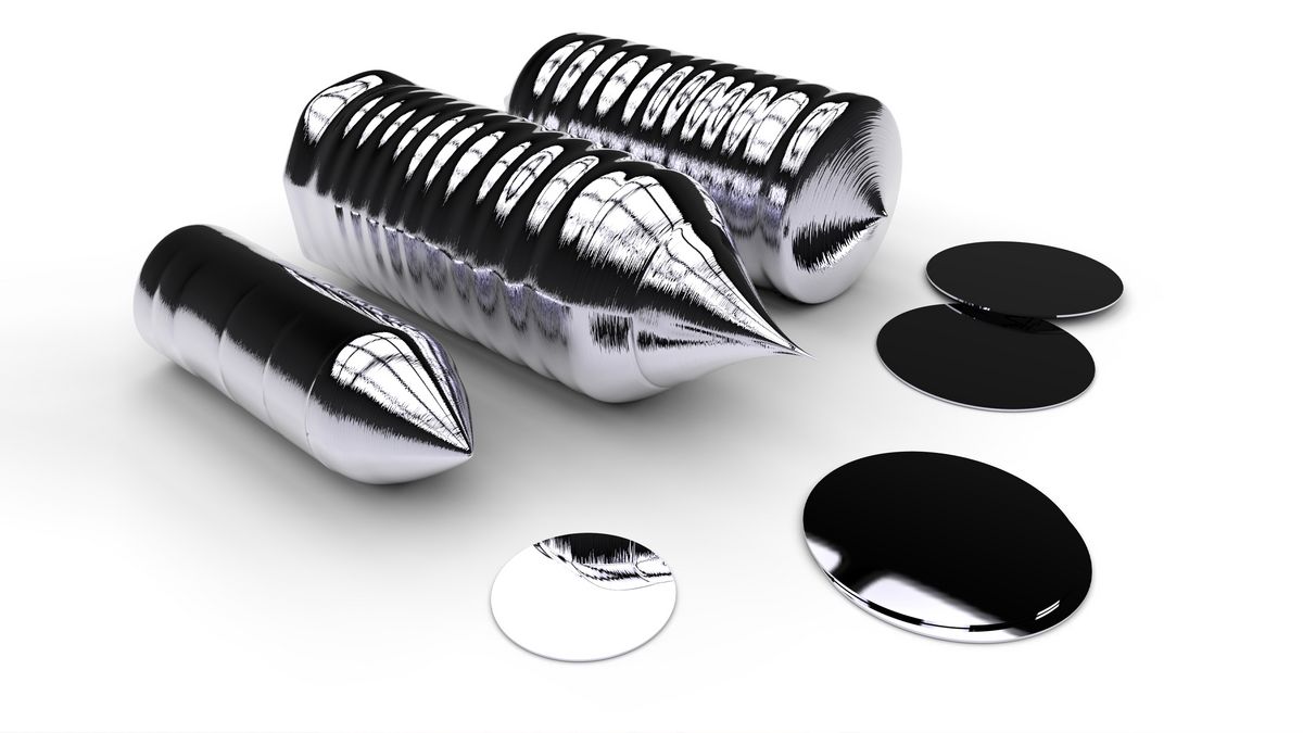
Now that we have our molten silicon hanging out in the crucible, we can add a seed crystal to promote the growth we want. When this crystal is slowly pulled back out, silicon atoms move to the bottom and combine to form what we’re looking for: a big cylindrical boule, or ingot, of pure silicon. The ingot is typically two or three feet in length and one foot in diameter.
Phil Wiss, regional sales manager for the Surface & Profile Division at UNITED GRINDING North America, describes the ingot as roughly the size and shape of a rugby ball. “The ingot is chemically pure, but highly anisotropic,” Wiss said. “In other words, the structural and electronic properties of the crystal vary drastically depending on their orientation. Also, you can’t predict the orientation of the crystal plane beforehand.”

For us at UNITED GRINDING, this is where the fun happens.
We make surface and profile, tool and cylindrical grinding machines that are known for their repeatable precision, and the semiconductor industry needs that precision like few other industries do.
THE STUDER SOLUTION
Because of the unpredictability of the ingot, it's hard to tell where grinding needs to happen to get the optimal chip performance. But integrated X-rays in STUDER cylindrical grinding machines take care of that, perfectly positioning the ingot for OD grinding.
THE BLOHM SOLUTION
That big silicon ingot has a dome at each end that, historically, would be cut off with a diamond saw. A decent saw costs somewhere in the ballpark of $2 million, and it takes somewhere between two and three hours to cut off the two-inch dome at each end of the ingot.
The PLANOMAT creep feed grinder tackles that two or three hour job in just 15 minutes. The time savings are incredible, as are the cost savings: the PLANOMAT costs less and does more than a diamond saw.


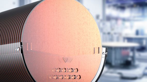
Hope you like wafers, because you’re getting a lot of them.
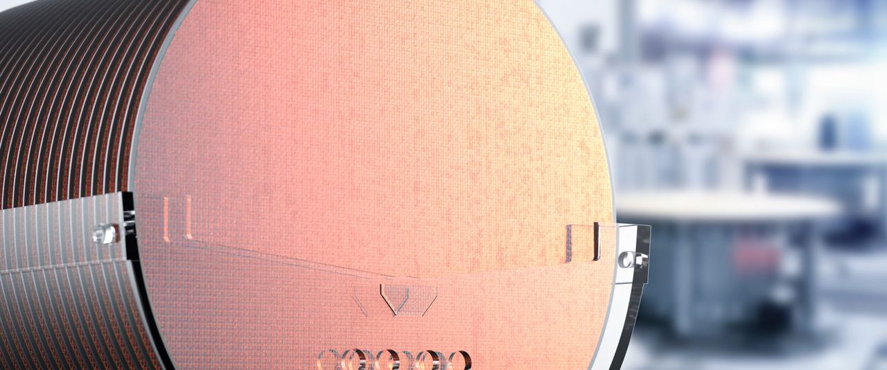
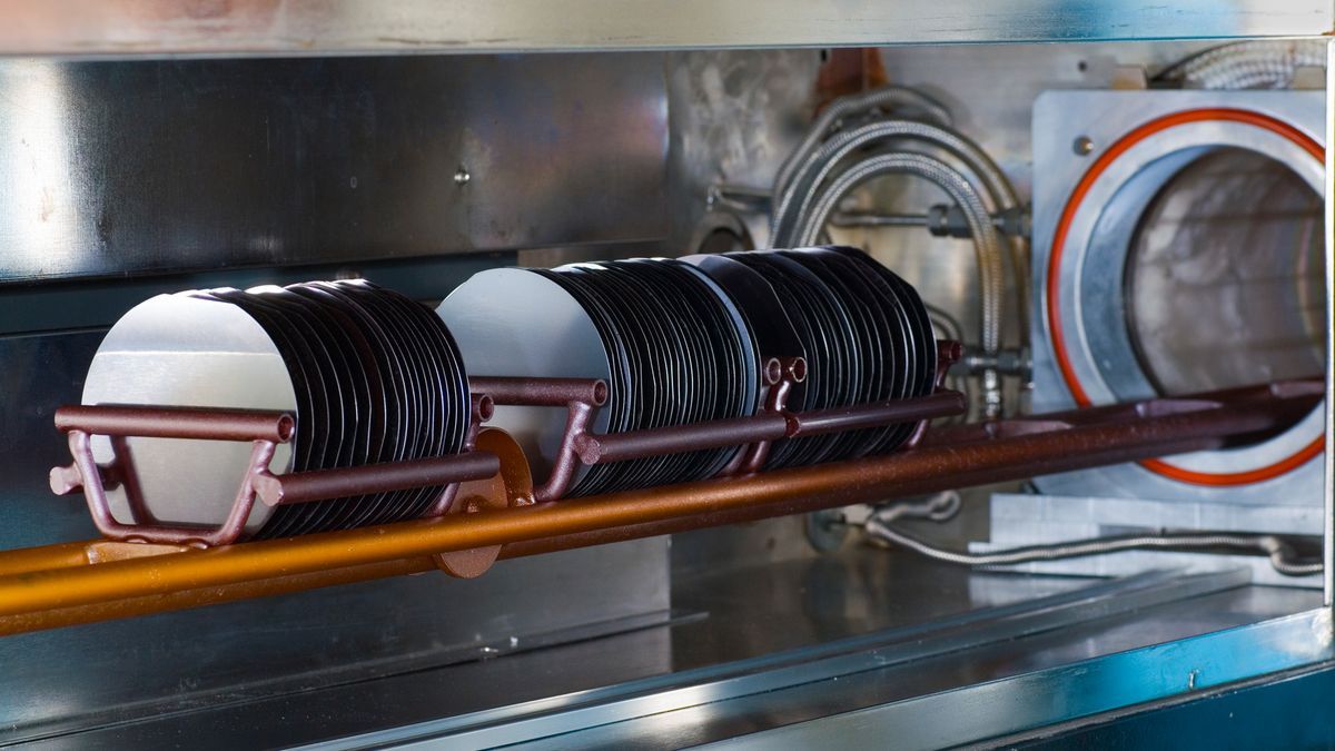
At this point, the dome-less ingot is turned into thin slices of wafer. Silicon wafers usually have diameters of about 12 inches, and in general, the bigger the wafer, the more microchips you can have.
It’s important to mention at this point that microchips are produced in sterile conditions, completely free of dust and debris. Just one lone particle of dust can ruin an entire microchip batch.


Next up: deposition, lithography, exposure and etching.
Now we’re getting to the point where microchip production moves past our area of expertise at UNITED GRINDING. First, a thin layer of silicon dioxide is grown on the wafer, after which the wafer is coated with photo-sensitive material.
Then, those prepared wafers make their way into a lithography machine where they’re exposed to UV light that contains the correct chip blueprint. The areas that were exposed to the UV light are hardened, while the unexposed areas are gassed away. The end result is the 3D microchip.
Finally, in the etching process, a thin metal such as aluminum acts as the bridge builder between the chip components. Each chip on the wafer is then tested for performance before it’s separated from its brothers and sisters.
Billions of transistors per chip, and we’re only just getting started.
The most advanced microchips on the planet (as of summer 2023) that are used for top-of-the-line graphics cards have somewhere in the neighborhood of 30 billion transistors per fingernail-sized chip. It boggles the mind.
Even more mind-boggling, according to Moore’s Law (which has impressively proven to be accurate decades later), chip manufacturing capability will double every two years or so.
In other words, growing microchips is one of humanity’s most impressive technological feats, indistinguishable from magic, and it’s nowhere near finished yet.
Okay, let’s go back to CNC grinding those silicon carbide ingots.
Before we adjourn, a quick reminder: UNITED GRINDING has incredibly efficient, powerful and precise surface, profile and cylindrical grinders that can make semiconductor manufacturers more productive than ever before.